


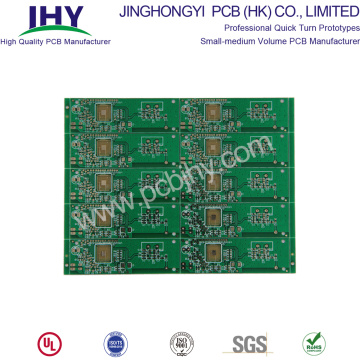
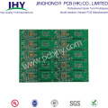


Low-cost 2 Layer PCB Prototype Multilayer PCB manufacturing
Product Description
With the development of high-tech, people need electronic products with high performance, small size and many functions, which make PCB manufacturing develop to light, thin, short and small. Limited space can realize more functions, wiring density will increase and aperture will be smaller. Double Sided PCB, or 2 layer PCB, came into being as the times require. From 1995 to 2005, the minimum pore size of mechanical drilling capacity decreased from 0.4 mm to 0.2 mm, or even smaller. The diameter of metallized pore is becoming smaller and smaller. The quality of the metallized holes on which the interlayer interconnection depends is directly related to the reliability of PCB.
For PCB manufacturers, the production of double-sided circuit boards is relatively easy, but in order to ensure the correctness of PCB design and the stability of terminal products, we also need to prototype the double-sided circuit boards to verify.
What is a double-sided PCB
Double-sided PCB has circuit boards on both front and back. It connects electrical performance through VIA through-hole. There are similarities and differences between blanking, forming and single-sided PCB. The lines of double-sided PCB are more dense, so we adopt exposure technology. The adhesion and gloss of solder barrier layer are brighter.
Manufacturing Technology of Double-sided PCB Board
Double-sided tin PCB/Immersion Gold PCB manufacturing process:
Cutting---drill hole---Immersion Copper---circuit---Pattern Plating---etching---Solder Mask---character---Spray tin (or Immersion Gold)---Edge of Gong-V-CUT (some boards don't need it)---Flying needle test---Vacuum packing
Double-sided gold-plated PCB manufacturing process:
Cutting---drill hole---Immersion Copper---circuit---Pattern Plating---Gold-plated---etching---Solder---character---Edge of Gong---V-CUT---Flying needle test---Vacuum packing
Multilayer Tin PCB/Immersion Gold PCB Manufacturing Process:
Cutting---Inner layer---Lamination---drill hole---Immersion Copper---circuit---Pattern Plating---etching---Solder---character---Spray tin (or Immersion Gold)-Edge of Gong-V-CUT---Flying needle test---Vacuum packing
Multilayer Gold-plated PCB Manufacturing Process:
Cutting---Inner layer---Lamination---drill hole---Immersion Copper---circuit---Pattern Plating---Gold-plated---etching---Solder---character---Spray tin (or Immersion Gold)-Edge of Gong-V-CUT---Flying needle test---Vacuum packing
In recent years, SMOBC and graphic electroplating are the typical processes for manufacturing double-sided metallized PCB. The process traverse method is also used in some special occasions.
I. Graphic Electroplating Process
CCL→Cutting→Punching reference hole→NC drilling→inspect→chip removing→Electroless copper plating→Electroplating Thin Copper→inspect→Printed Circuit Board→Film (or screen printing)→Exposure development (or curing)→Inspection repair board→Graphic plating(Cu+Sn/Pb)→Removing membrane→etching→Inspection repair board→Plug Nickel-plated and Gold-plated→Hot melt cleaning→Electrical on-off detection-->Cleaning treatment→Screen Printing Resistance Welding Graphics→Solidification→Screen Printing Marking Symbol→Solidification→Shape Processing→Cleaning and drying→test→Packing→Finished products.
In the process, "electroless copper plating---electroless copper plating" two processes can be replaced by "electroless copper plating thick" one process, both of which have their advantages and disadvantages. Graphic electroplating-etching double-sided-hole metallized sheet is a typical process in the 1960s and 1970s. In the mid-1980s, bare copper cladding resistance coating (SMOBC) technology gradually developed, especially in the precision double panel manufacturing has become the mainstream technology
2. SMOBC process
The main advantage of SMOBC board is to solve the short-circuit phenomenon of solder bridging between thin wires. At the same time, due to the constant ratio of lead to tin, SMOBC board has better solderability and storage than hot-melt plate.
There are many methods to manufacture SMOBC board, such as standard pattern electroplating subtraction method and SMOBC process; subtraction pattern electroplating SMOBC process using tin plating or tin dipping instead of electroplating lead and tin; blocking or masking hole SMOBC process; additive SMOBC process, etc. The SMOBC process of pattern electroplating for lead and tin removal and the SMOBC process of plugging method are mainly introduced below.
The SMBC process of pattern electroplating and lead and tin stripping is similar to that of pattern electroplating. Change occurs only after etching.
Double-sided copper clad foil - > from graphic plating process to etching process - > lead and tin removal - > inspection - > cleaning - > solder resistance graphics - > plug nickel plating - > plug tape - > hot air leveling - > cleaning - > screen printing marking - > shape processing - > cleaning and drying - > finished product inspection - > Packaging - > finished products.
3. The main technological process of the plugging method is as follows:
Double-sided foil clad sheet - > drilling - > electroless copper plating - > blocking - > screen printing imaging - > etching - > screen printing material, blocking material - > cleaning - > welding pattern - > plug nickel plating, gold plating - > plug sticking tape - > hot air leveling - > the following procedure is the same to the finished product.
The technological steps of this process are simple, and the key is to plug the hole and clean the ink for plugging the hole.
In the process of blocking hole, if we do not use blocking ink blocking hole and screen printing imaging, but use a special masking dry film to cover the hole, and then expose it to make a positive image, this is the process of masking hole. Compared with the plugging method, it no longer has the problem of cleaning ink in the hole, but has higher requirements for masking dry film.
SMOBC process is based on the production of bare copper-hole metallized double panels and the application of hot air leveling process.
Detailed parameters of 2 layer PCB Prototype in display
| Base Material | FR4 |
| Board Thickness | 1.6mm±10% |
| Copper Weight | 1oz |
| Surface Finish | Immersion Tin |
| Minimum Trace Width/Spacing | 0.15/0.15mm(6/6mils) |
| Solder Mask Color | Green |
| Silkscreen Color | White |
| Flame Retardant Properties | 94 V-0 |
| Application | Consumer Electronics |
The difference between two-sided PCB and one-sided PCB
The difference between one-sided PCB and two-sided PCB is the number of copper layers. Double-sided circuit boards have copper on both sides of the circuit board, which can be connected through a through-hole connection. There is only one layer of copper on one side and only a simple circuit can be used. The holes can only be used for plug-ins that cannot be opened. The technical requirement of double-sided circuit board is to increase wiring density, smaller aperture and smaller metallized aperture. The quality of interconnected metal holes depends on the reliability of printed circuit boards. With the shrinkage of pore size, the original impurities, such as grinding debris and volcanic ash, which have no effect on larger pore size, will remain in the small pore, which will lead to the loss of chemical copper and copper plating.
2 layer PCB prototype assembly method
In order to ensure the reliable conductive effect of double-sided PCB, the connecting holes of double-sided PCB (i.e. the through holes of metallization process) should be welded with wires first, and the protruding part of the connecting wire tip should be cut off to avoid the operator's hand being injured. This is the wiring preparation of PCB.
1. For the equipment that needs to be moulded, the process should be processed according to the requirements of the process drawings; that is to say, the plug-in is first moulded.
2. After forming, the model surface of the diode should be upward, and there should be no inconsistent two pins between the lengths.
3. When inserting equipment with polarity requirements, it should be noted that polarity should not be reversed. Rollers are integrated with block components. After inserting the instrument, the device should not be tilted vertically or flat.
4. The power of soldering iron for welding is 25-40W. The temperature of soldering head should be controlled at about 242 C. The temperature is too high, the head is easy to "die". The solder cannot melt at low temperature. Welding time is controlled in 3-4 seconds.
5. Normal welding is generally operated according to the principle of welding equipment from short to high and from inside to outside. Welding time should be mastered. If welding time is too long, the copper wire plate on copper wire will be burned.
6. Because it is double-sided welding, it should also be used as a process framework for placing circuit boards, etc. to avoid tilting equipment.
7. After the welding of the circuit board is completed, a comprehensive inspection should be carried out to check the location of the leakage welding. After confirmation, the pins of the redundant components of the circuit board are trimmed and then flowed into the next process.
8. In specific operations, the welding quality of products should be ensured in strict accordance with the relevant process standards.
Product Categories : PCB Prototype